Bare Board Printed Circuit Boards - Absolute Electronics


![» Introduction to PCB Design July 11 / PCB电路板设计入门 7月11号 新车间 [XinCheJian]](/img/GGqFzZBf-how-is-a-pcb-made.png)


About How Is
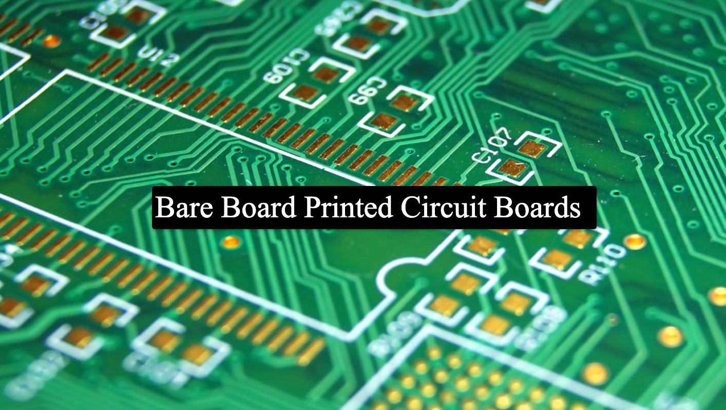
A Printed Circuit Board PCB is a flat board made from an insulating material of some kind. Usually, they are made from fiberglass, but other materials can be used as well. PCBs also have thin layers of conductive material etched into the surface. These conductive material layers are called 'traces' and are usually made from either copper or
The PCB manufacturing process begins with blueprints, goes through a complex multi-stage manufacturing stage, and ends on a functional PCB. Each step is vital and builds on earlier steps of the process, and this is why when discussing how are PCBs manufactured, we need to have a holistic picture of the process as a whole.
PCB Manufacturing Process Flowchart - Step by Step Step-1 Patterning or Etching Majority of printed circuit boards are manufactured by applying a layer of copper over the entire surface of the PCB substrate material either on one side or both sides. This creates a blank printed circuit board, with the copper everywhere on the surface.
The PCB Manufacturing Process A printed circuit board, or PCB, is a non-conductive material with conductive lines, also called traces, printed or etched into the base. Electrical components are mounted on the board, with traces connecting the components to form a working circuit.
This step in PCB manufacturing prepares to make actual PCB. The basic form of PCB comprises a laminate board whose core material is epoxy resin and glass fiber that are also called substrate material.
The PCB manufacturing process is a complex yet fascinating journey that combines advanced technology, precision engineering, and rigorous quality control. From design to final inspection, each step plays a critical role in ensuring the reliability and performance of the finished product.
Explore our comprehensive guide on the step-by-step process of how PCBs are manufactured, from the initial design stages to the final production.
The PCB manufacturing process is a complex and multi-step journey that transforms a design concept into a functional electronic component. Each step, from design and material selection to final testing and inspection, plays a critical role in ensuring the production of high-quality, reliable, and efficient PCBs.
At its core, a Printed Circuit Board PCB is a flat board made of insulating material, typically fiberglass, with conductive pathways etched or printed onto its surface. These pathways, known as traces, connect electronic components like resistors, capacitors, and integrated circuits, enabling them to work together as a cohesive system. The Basic Structure of a PCB A standard PCB consists of
Introduction to PCBs A printed circuit board PCB is a laminated board made of non-conductive substrate material with conductive pathways etched from copper sheets and laminated onto the substrate. PCBs allow electrical components like resistors, capacitors, integrated circuits, and others to be mechanically supported and electrically connected using conductive tracks, pads, and other